SK hynix Flags Data Movement Between Memory Tiers as SI's New Bottleneck; 3D Stacked DRAM and High-Bandwidth Flash Join the Roadmap
SEOUL — The bottleneck in SI infrastructure has shifted from the gap between compute and memory to data movement between memory tiers themselves, SK hynix President and Chief Development Officer Ahn Hyun said in a keynote at the 28th Semiconductor Exhibition (SEDEX 2026), which opened on October 14 at COEX in Seoul. He proposed connecting the entire memory hierarchy densely through 3D stacked DRAM and high-bandwidth flash (HBF).
3D stacked DRAM places DRAM dies directly on top of logic dies such as GPUs and NPUs, bonded vertically through silicon vias — a departure from today's 2.5D packaging, where data moves laterally through an interposer. By shortening the data path, Ahn said, I/O terminals can be increased by tens of times compared with HBM, maximizing bandwidth while sharply cutting power consumption.
HBF transplants HBM's stacking technology onto NAND flash, offering roughly half the bandwidth of same-generation HBM at more than ten times the capacity. SK hynix is driving HBF standardization with partners including SanDisk and has released version 0.7 of the specification through the Open Compute Project: up to 512GB capacity, 0.4 to 3.0 TB/s of bandwidth by grade, and a UCIe chiplet interface. The company targets a final specification in early 2027 and "HBF Cube" samples in early 2028. Ahn noted that writes make up an extremely small share of SI inference workloads, sidestepping NAND's endurance limits, while prefetching addresses its latency.
On current products, SK hynix began volume supply of HBM4 in the second quarter of this year, and its 12-high HBM4E samples shipped to key customers in June offer 48GB capacity at up to 16 Gb/s per pin; the company plans to raise the share of customized HBM across the HBM4E and HBM5 generations. It is also building CXL-based pooled memory and has completed conceptual design with major technology companies for "Storage Next" SSDs that redesign internal architecture for four to eight times today's IOPS.
At the system level, Vice President Kim Ho-sik presented the Memory-Centric AI Rack System (MARS) at the OCP Global Summit in San Jose on October 12: memory is disaggregated from CPUs and GPUs into a large shared pool allocated on demand. In multi-turn SI agent inference tests, SK hynix said, MARS improved time to first token by three to five times versus recomputation approaches. Ahn projected that SI infrastructure performance scale will expand to roughly 19 to 20 times 2026 levels by 2030, driven by complex reasoning, longer contexts and more inference requests per second.
SK hynix ranks No. 3 in GSM's Global Chip Company Rankings on 2025 revenue, and holds about 50% of HBM revenue, the world's largest share (TrendForce, Q2 2026).
Published by GSM · USA (original Chinese edition)
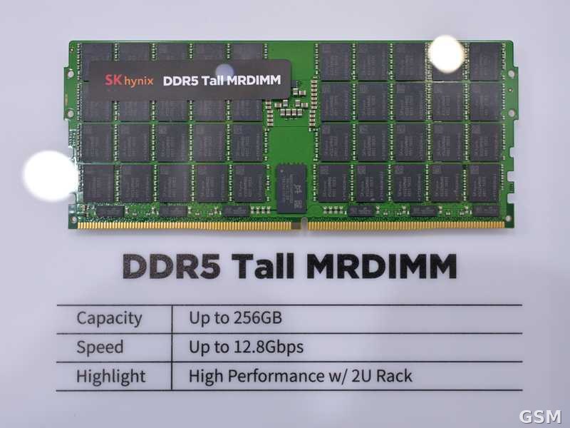
Photo: 图:SK 海力士 DDR5 Tall MRDIMM 内存产品展示。照片:4300streetcar,CC BY 4.0,经 Wikimedia Commons。Photo: SK hynix DDR5 Tall MRDIMM modules on display. Photo: 4300streetcar, CC BY 4.0, via Wikimedia Commons.