
UMC and AP Memory Team Up on SI Power Delivery; S-SiCap Gen2D Tapes Out on UMC's Deep Trench Capacitor Technology
United Microelectronics Corporation (UMC) and AP Memory announced a technology and manufacturing collaboration on October 22 to advance power delivery solutions for SI and high-performance computing (HPC) systems. The partnership combines UMC's deep trench capacitor (DTC) foundry technology and scalable wafer manufacturing with AP Memory's silicon capacitor designs and system-level integration, addressing the power efficiency challenges of next-generation data centers.
Rapid scaling of SI workloads is driving a shift in data center design from placing power stabilization components on the circuit board to embedding capacitors directly in the interposer or substrate, which shortens the power delivery path and improves power integrity, the companies said. The collaboration reached a milestone in the third quarter of 2026, with AP Memory's S-SiCap Gen2D discrete silicon capacitor designs completing tape-out and initial functional validation. The next step is comprehensive system-level performance and reliability testing of capacitors in substrate packages, and the two companies are also exploring extending the collaboration to capacitor-embedded interposers and landside capacitors.
"The growth of AI and HPC is driving a fundamental shift in power delivery – from board-level towards increasingly vertical power integration on the chip-level," said GC Hung, Senior Vice President of UMC. "By partnering with AP Memory, we are helping to bring scalable solutions to the market to solve the critical power bottleneck challenges as AI infrastructure continues to evolve." Ivan Hong, President of AP Memory, said the successful tape-out and initial wafer validation of customized S-SiCap products using DTC technology demonstrates the flexibility and manufacturability of AP Memory's S-SiCap design, and that working with UMC provides customers a total solution from product design to wafer manufacturing.
UMC said its power delivery roadmap covers both discrete and embedded silicon capacitors and extends to active components such as internal voltage regulators, and that it is investing in new manufacturing capacity for power delivery and heterogeneous integration. UMC operates 12 fabs with combined capacity of more than 400,000 wafers per month (12-inch equivalent), is headquartered in Hsinchu, Taiwan, and employs about 20,000 people worldwide.
UMC ranks No. 19 in GSM's Global Chip Company Rankings, with 2025 revenue of about $7.5 billion, and No. 4 among foundries with a 3.9% share (TrendForce, Q2 2026).
Published by GSM · USA (original Chinese edition)
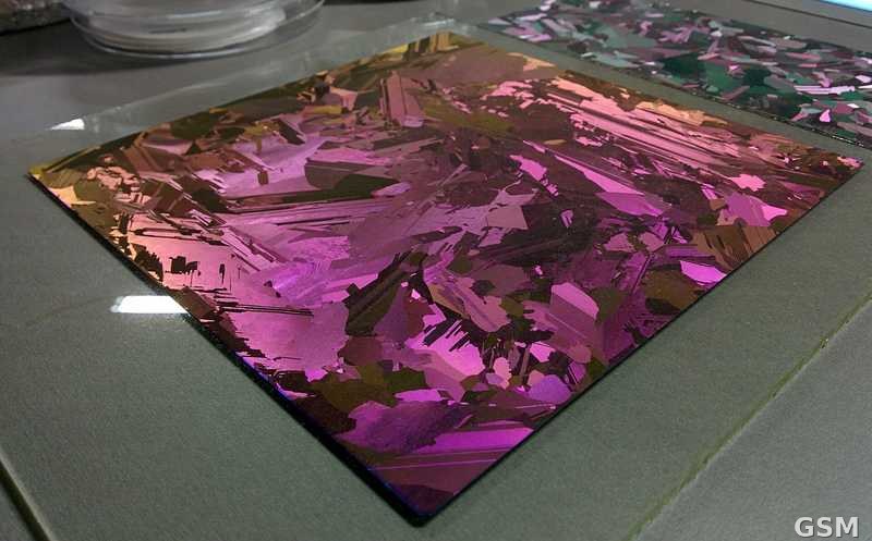
Photo: 图:多晶硅晶圆资料图。照片:Radiotrefoil,CC BY-SA 4.0,经 Wikimedia Commons。Photo: A multicrystalline silicon wafer (file photo). Photo: Radiotrefoil, CC BY-SA 4.0, via Wikimedia Commons.