
IBM and Siemens Announce a Nanostack Transistor Research Partnership on November 13: The Current 7 Angstrom Node Packs Nearly 100 Billion Transistors Into a Fingernail-Sized Area
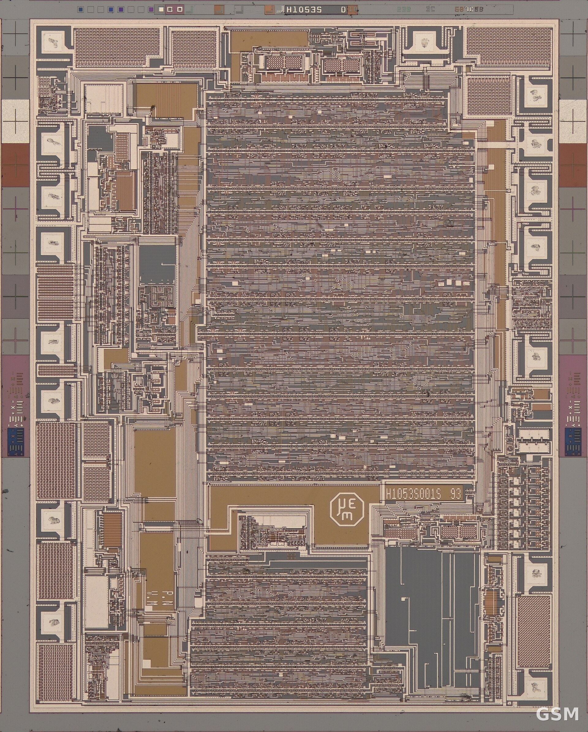
IBM and Siemens announced a research partnership on November 13, 2026 to advance IBM's three-dimensional nanostack transistor design beyond the 7 angstrom node. Nanostack is a three-dimensional, nanosheet-based design that vertically stacks and staggers transistors. The work focuses on the design, simulation and lithography techniques needed for nanostack generations beyond the current node. At its current 7 angstrom node, nanostack packs nearly 100 billion transistors into a space the size of a fingernail, and allows different material combinations within each stacked layer, according to the announcement. The two companies will develop advanced virtual models of nanostack to model performance and address fabrication challenges before chips are built. IBM unveiled the nanostack architecture earlier in 2026 and demonstrated its viability. The announcement does not state the performance gains expected from the design or when the next node will be reached. The architecture is designed to support the logic scaling needed for AI and other emerging technologies over the coming decade.
(Source: IBM)
Source: IBM
Published by GSM · USA (original Chinese edition)
Photo: 图:集成电路芯片裸片微距特写。Phiarc,CC BY-SA 4.0,经 Wikimedia Commons。 / Photo: Phiarc, CC BY-SA 4.0, via Wikimedia Commons.
 Silicon Carbide Nanomaterials in Disc Brake Pads: 0.5% Loading Raised Average Brake Force by Up to 19%, With Fade Resistance Up to 130°C2026-11-14
 PEBA-PEMA Blend Membrane Separates 1-Butanol With Flux of 0.19 kg/m2/h and Separation Factor of 15.5 at 5 Percent PEMA, Published in Scientific Reports on November 132026-11-14