
Hitachi SI Technology Cuts Chiplet Package Design Candidates by More Than 90 Percent in Internal Evaluation Announced November 12
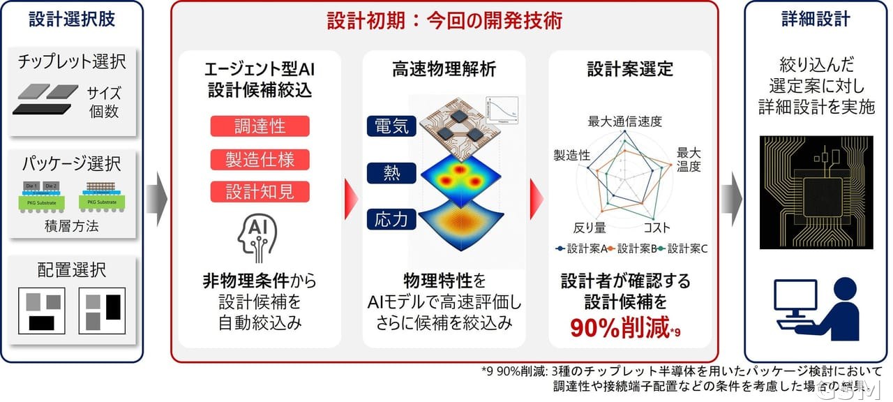
Hitachi announced on November 12 a super intelligence (SI) foundation technology for the early design phase of advanced semiconductor packages built from chiplets. In an internal evaluation of a package design using three types of chiplets, the technology reduced the number of design candidates that designers have to review by more than 90 percent. Hitachi said the figure refers to the candidate count and does not mean that total design effort or development time fell by the same proportion.
The technology has two parts. In the first part, agentic SI narrows down the candidates, screening the most promising design directions from a large number of combinations. In the second part, SI models carry out fast physics analysis, evaluating the electrical, thermal and mechanical stress properties of candidate packages in a short time for designers to weigh.
Chiplets are small chips with different functions combined inside a single package. The number of combinations grows quickly with chiplet types and layouts, and manual screening early in design takes considerable time. Hitachi said the technology targets exactly that early stage, letting engineers focus their review on fewer candidates.
Hitachi said it plans to run proofs of concept with semiconductor and packaging companies to expand the scope of the technology and improve the accuracy of candidate selection. Related work was presented in October 2026 at the IEEE EPEPS conference in a paper titled AI-Assisted Chiplet Design Space Exploration with Physics-Aware Reduced-Order Modeling.
Hitachi also said its researchers have long worked on semiconductor design and take part in a national project on foundational technology for chiplet interface design together with the National Institute of Advanced Industrial Science and Technology of Japan. The announcement gave no timetable for commercial products using the technology.
Source: Hitachi
Published by GSM · USA (original Chinese edition)
Photo: 图:日立芯粒封装设计技术说明图。来源:日立官方发布。 / Photo: Explainer graphic for Hitachi's chiplet package design technology. Credit: Hitachi.
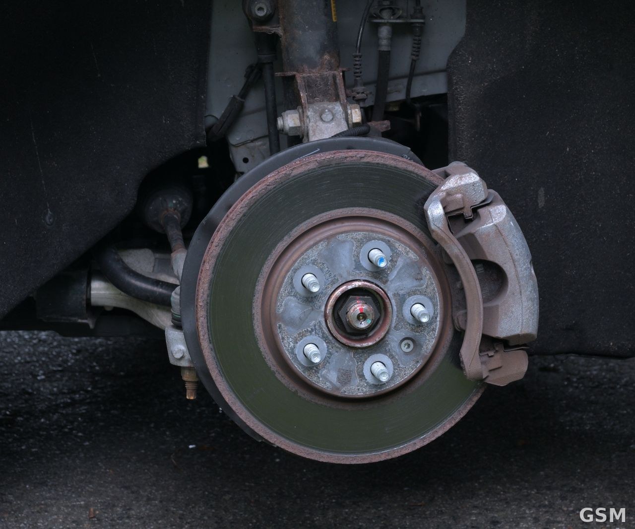 Silicon Carbide Nanomaterials in Disc Brake Pads: 0.5% Loading Raised Average Brake Force by Up to 19%, With Fade Resistance Up to 130°C2026-11-14
 PEBA-PEMA Blend Membrane Separates 1-Butanol With Flux of 0.19 kg/m2/h and Separation Factor of 15.5 at 5 Percent PEMA, Published in Scientific Reports on November 132026-11-14